josuah.net | panoramix-labs.fr
Transistors are built so that you can control electrons flowing through them in some way. But that model ie rarely explained
A transistor permits to control a current going through two pins, using the 3rd pin as an interruptor: They are like resistor whose resistance is chosen by an input signal.
This permits to combine them in order to:
By the effect of the control input signal, the transistor is either:
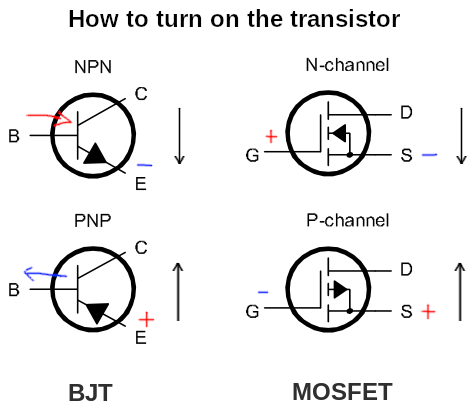
For BJT (pnp, npn) the control input signal is a current.
They have a great linearity: the output letting some, but not all current flow: allows proportional control of the output current according to the input signal.
For MOSFET (depletion, enhancement) the control input signal is a voltage.
They do not have a great linearity: they are used as on/off switches. To have something intermediate, they can be turned on and off repeatedly, i.e. with a PWM input control signal.
                    BJT         MOSFET

Control pin         (B)ase      (G)ate

Reference pin       (E)mitter   (S)ource

Target pin          (C)ollector (D)rain
The control pin (base/gate) decides the state ON/OFF of the transistor.
The charges move from the reference pin (emitter/source) to the target pin (collector/drain)
To turn the transistor ON, the control pin (base/gate) must have a more positive voltage than the reference pin (emitter/source).
The charges moving from the reference (emitter/source) to the target (collector/drain) are (**n**)egative.
So the conventional current moves from collector/drain to emitter/source.
To turn the transistor ON, the control pin (base/gate) must have a more negative voltage than the reference pin (emitter/source).
The charges moving from the reference (emitter/source) to the target (collector/drain) are (**p**)ositive.
Same for conventional current.
On the symbols, the arrow is always shown connected to the reference pin (emitter/source),
It is a global representation about how to use the component.
The arrow has the direction of the conventonal current (though MOSFETs are voltage-controlled) as used to turn the transistor ON.
MOSFET have an additional detailed view which shows the internals. This is this view which is almost always used for MOSFETs
The arrow has the direction of the electrons, opposite of the conventional currents, as used to turn the transistor OFF.
Other kinds of semiconductors are not discussed here: JFET, UJFET, TRIACs...
Only enhancement MOSFETs are discussed here. Their counterpart are depletion MOSFETs, normally ON but turned OFF by a stronger signal on the gate.
There we go! Why do textbooks so rarely say those things clearly? Some short, interesting resources that help: