josuah.net | panoramix-labs.fr
For my SDR project, I want to combine a RP2040 and an ICE40.
Both a are widely available board and cover a lot of features together.
The RP2040 features would be expensive to do in an FPGA:
An FPGA complements quite well what the RP2040 lacks:
Let's see if we can make that work in practice...
SPI comes with its own clock signal. It is convenient and reliable to use it as clock for the SPI core: @(posedge spi_clk) in Verilog instead of the @(posedge wb_clk_i) clock used by the rest. This means we have now two clock domains and need to plan cooperation between them.
This introduce me to the famous topic of Clock Domain Crossing: taking data from one clock domain to another.
Recommandations often encountered is to use a handshake protocol. I will stick to the simplest implementation I can come-up with and see if it works well in practice.
Simple handshake protocol for crossing clock domain.
handshake_ack (and reads handshake_req).handshake_req (and reads handshake_ack).: : : : : : : : : : : : __:_______________:_______________:______________ handshake_data __X_______________X_______________X______________ : _______________: : : : __________ handshake_req ______/ : : : \_______________/ : : : : : :_______________: : : : :__ handshake_ack ______________/ : : : \_______________/ : : : : : : : : : : : : (1) (2) (3) (4) (1) (2) (3) (4) (1) (2) (3) (4)
handshake_data to the data to transfer (1) then invert handshake_req (2).handshake_data to a local register (3) then sets handshake_ack to the same value as handshake_req (4).The Wishbone protocol uses many more wires than SPI for communicating, so a wire protocol for encoding Wishbone over another transport is required.
Here is what I came-up with, inspired by spibone.
Wishbone read transaction:
MCU   W000SSSS AAAAAAAA :::::::: :::::::: :::::::: :::::::: :::::::: ::::::::
      │   ├──┘ ├──────┘
FPGA  │:::│::: │::::::: 11111111 00000000 DDDDDDDD DDDDDDDD DDDDDDDD DDDDDDDD
      │   │    │        ├──────┘ ├──────┘ ├─────────────────────────────────┘
      WE  SEL  ADR      WAIT     ACK      DAT
Wishbone write transaction:
MCU   W000SSSS AAAAAAAA DDDDDDDD DDDDDDDD DDDDDDDD DDDDDDDD :::::::: ::::::::
      │   ├──┘ ├──────┘ ├─────────────────────────────────┘
FPGA  │:::│::: │::::::: │::::::: :::::::: :::::::: :::::::: 11111111 00000000
      │   │    │        │                                   ├──────┘ ├──────┘
      WE  SEL  ADR      DAT                                 WAIT     ACK
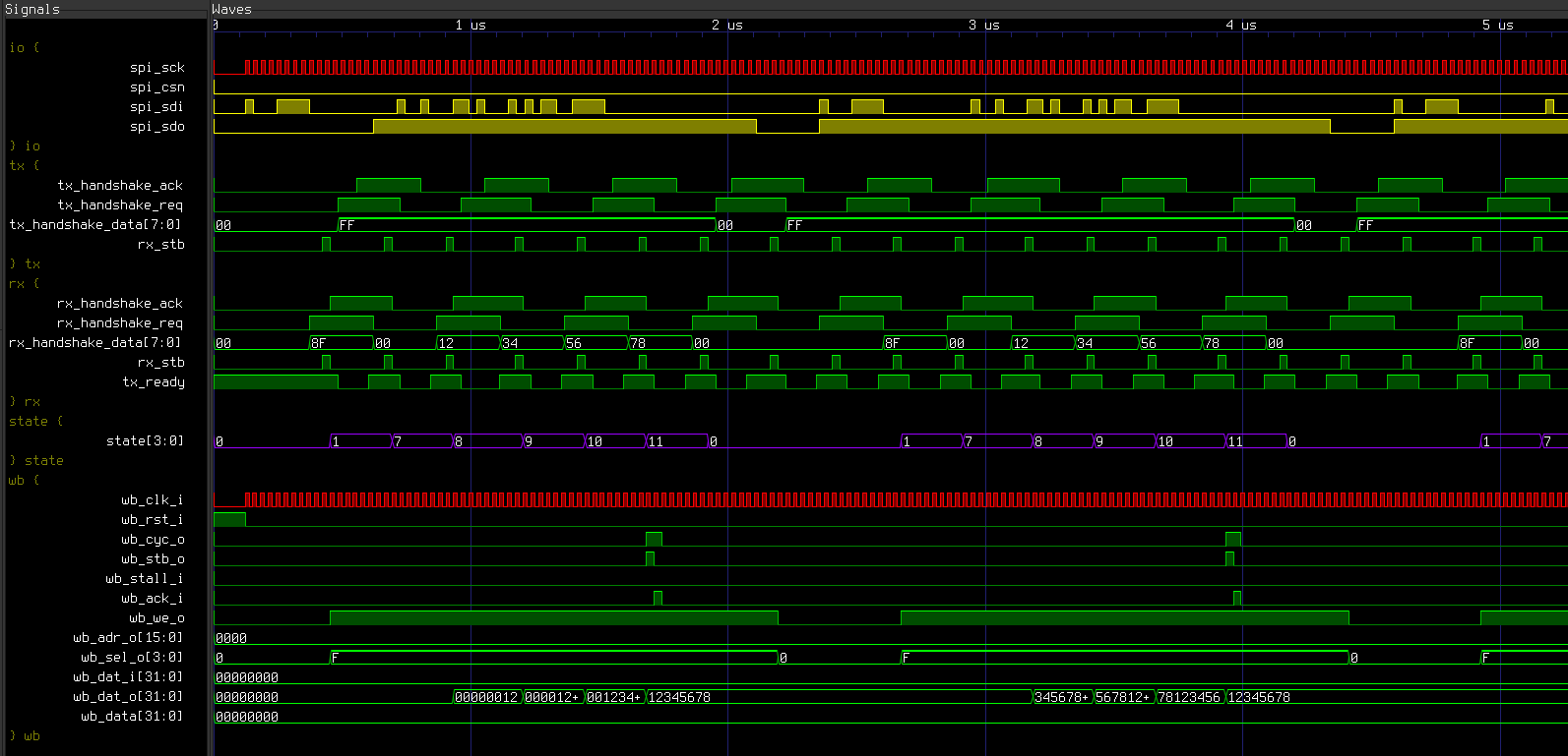
While far from battle-tested, this seems to work at least a little:
This is the state of the signals on the FPGA, with the clocks in red, the I/O signals in yellow, and the others in green, with the global state in violet.
The I/O block shows the clock from the MCU (or rather here, simulation), that are captured by the rx{} block as packets in handshake_data (8'h8F, 8'h00, 8'h12, ...),
These are then decoded by the state machine shown in state, and finally sent to the bus.
We can recognize the data payload 32'h12345678 sent packet per packet on spi_sdi.